Discontinued On Mar. 2017
VT-RNSII
Inline PCB Inspection System
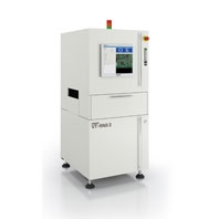
For Even More Efficient SMT Production Introducing the 2nd Generation RNS Series
* Information in this page is a reference that you created on the basis of information in the product catalog before the end of production, may be different from the current situation, such as goods for / supported standards options / price / features of the product. Before using, please check the compatibility and safety system.
Related Contents
- Features
- Lineup
- Specifications
- Dimensions
- Catalog / Manual / CAD / Software
last update: August 1, 2013
Caution: This product may cause interference if used in residential areas.
Hardware Configuration
| M size | L size | ||
|---|---|---|---|
| P/Z/S | |||
| Image signal
input unit |
Camera | 3-CCD camera | |
| Illumination | Ring-shaped LEDs (R, G, B) | ||
| Image resolution | 10, 15, 20 μm | ||
| Main unit | Feed method | Belt | |
| Line height | 900 ±15 mm | ||
| PCB carrier width
adjustment |
Automatic | ||
| PCB fixing method | Outer frame | ||
| Power supply | AC 100/115 V /120 V/200 V/220 V/230 V/240 V ±10% (single phase) | ||
| Air | 0.4 to 0.6 Mpa | ||
| Ambient operating temperature | +10 to +35°C | ||
| Ambient operating humidity | 35 to 80% RH (with no condensation) | ||
| Weight | Approx. 500 kg | Approx. 650 kg | |
| Dimensions | 700 (W) × 900 (D) × 1,600 (H) mm
(Excluding Patlite signal tower) |
920 (W) × 1,365 (D) × 1,600 (H) mm
(Excluding Patlite signal tower) |
|
Functional Specifications
| M size | ||||
|---|---|---|---|---|
| P | Z | S | ||
| Inspectable
PCBs |
Type | Post-printing | Post-placement
(before reflow) |
Post-reflow |
| Dimensions | 50 (W) × 50 (D) to 333 (W) × 255 (D) mm | |||
| Thickness | 0.3 to 2.5 mm | |||
| Clearance | Above PCB: 20 mm (0.79 in) (standard), 40 mm (1.57 in) (optional)
Below PCB: 40 mm (1.57 in) |
|||
| Inspection items | Presence of solder,
insufficient/excessive solder, solder shifting, grazing, bridging, spreading, leaking |
Presence of solder,
component shifting, polarity error, missing components, wrong components, solder balls, skewing, bridging, foreign objects |
Presence of solder, wrong
components, missing components, bridging, lifting, component shifting, fillets, wettability, lead bending, adhesive, solder balls |
|
| Number of inspection points | 40,000 lands/PCB max. | 10,000 components/PCB max. | ||
| Data storage | Computer hard disk | |||
| Component-specific
inspection data library |
Component types, groups, variations | |||
| Inspection result output | PCB name, PCB ID, component name, type of fault, etc. | |||
| Communications | Ethernet, RS-232C | |||
| PCB feed mode | Through, turnback | |||
| Reference position | PCB feed direction: left or right (selected at shipment);
Longitudinal: Front or back (selected at shipment) |
|||
| L size | ||||
|---|---|---|---|---|
| P | Z | S | ||
| Inspectable
PCBs |
Type | Post-printing | Post-placement
(before reflow) |
Post-reflow |
| Dimensions | 80 (W) × 50 (D) to 510 (W) ×460 (D) mm
80 (W) × 110 (D) to 510 (W) ×460 (D) mm (with PCB warpage correction unit) |
|||
| Thickness | 0.3 to 3.0 mm | |||
| Clearance | Above PCB: 20 mm (0.79 in) (standard), 40 mm (1.57 in) (optional)
Below PCB: 50 mm (1,97 in) |
|||
| Inspection items | Presence of solder,
insufficient/excessive solder, solder shifting, grazing, bridging, spreading, leaking |
Presence of solder,
component shifting, polarity error, missing components, wrong components, solder balls, skewing, bridging, foreign objects |
Presence of solder, wrong
components, missing components, bridging, lifting, component shifting, fillets, wettability, lead bending, adhesive, solder balls |
|
| Number of inspection points | 40,000 lands/PCB max. | 10,000 components/PCB max. | ||
| Data storage | Computer hard disk | |||
| Component-specific
inspection data library |
Component types, groups, variations | |||
| Inspection result output | PCB name, PCB ID, component name, type of fault, etc. | |||
| Communications | Ethernet, RS-232C | |||
| PCB feed mode | Through, turnback | |||
| Reference position | PCB feed direction: left or right (selected at shipment);
Longitudinal: Front or back (selected at shipment) |
|||
last update: August 1, 2013
 Product Category
- Inspection System
-
PCB Inspection System
-
Discontinued
- VT-RNSII
-
Discontinued
-