CJ1W-OC / OA / OD
CJ-series Output Units
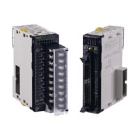
A Wide Range of Basic Output Units for High Speed Output and Different Applications. This unit is available for CJ/NJ controller.
Related Contents
- Features
- Lineup
- Specifications
- Dimensions
- Catalog / Manual / CAD / Software
last update: April 1, 2025
CJ1W-OC201 Contact Output Unit (Independent Relays, 8 Points)
| Name | 8-point Contact Output Unit with Terminal Block (Independent Relays) |
|---|---|
| Model | CJ1W-OC201 |
| Max. Switching Capacity | 2 A 250 VAC (cosφ = 1), 2 A 250 VAC (cosφ = 0.4), 2 A 24 VDC (16 A/Unit) |
| Min. Switching Capacity | 1 mA 5 VDC |
| Relays | NY-24W-K-IE (Fujitsu Takamizawa Components, Ltd.), Cannot be replaced. |
| Service Life of Relay | Electrical: 150,000 operations (24 VDC, resistive load)/100,000 operations (240 VAC, cosφ
= 0.4, inductive load) Mechanical: 20,000,000 operations Service life will vary depending on the connected load. |
| ON Response Time | 15 ms max. |
| OFF Response Time | 15 ms max. |
| Number of Circuits | 8 independent contacts |
| Insulation Resistance | 20 MΩ between external terminals and the GR terminal (500 VDC) |
| Dielectric Strength | 2,000 VAC between the external terminals and the GR terminal for 1 minute at a leakage
current of 10 mA max. |
| Internal Current
Consumption |
90 mA 5 VDC max.
48 mA 24 VDC max. (6 mA × No. of ON points) |
| Weight | 140 g max. |
| Circuit Configuration |
 The device variable names are the names that use "Jxx" as the device name. |
| External connection and
terminal-device variable diagram |
 The device variable names are the names that use "Jxx" as the device name. The input power supply polarity can be connected in either direction. |
* Terminal numbers A0 to A8 and B0 to B8 are used in the external connection and terminal-device variable diagrams.
They are not printed on the Units.
Note: Although 16 I/O bits (1 word) are allocated, only 8 of these can be used for external I/O.
They are not printed on the Units.
Note: Although 16 I/O bits (1 word) are allocated, only 8 of these can be used for external I/O.
CJ1W-OC211 Contact Output Unit (16 Points)
| Name | 16-point Contact Output Unit with Terminal Block |
|---|---|
| Model | CJ1W-OC211 |
| Max. Switching Capacity | 2 A 250 VAC (cosφ = 1), 2 A 250 VAC (cosφ = 0.4), 2 A 24 VDC (8 A/Unit) |
| Min. Switching Capacity | 1 mA 5 VDC |
| Relays | NY-24W-K-IE (Fujitsu Takamizawa Components, Ltd.), Cannot be replaced. |
| Service Life of Relay | Electrical: 150,000 operations (24 VDC, resistive load)/ 100,000 operations (250 VAC,
cosφ = 0.4, inductive load) Mechanical: 20,000,000 operations Service life will vary depending on the connected load. |
| ON Response Time | 15 ms max. |
| OFF Response Time | 15 ms max. |
| Number of Circuits | 16 points/common, 1 circuit |
| Insulation Resistance | 20 MΩ between external terminals and the GR terminal (500 VDC) |
| Dielectric Strength | 2,000 VAC between the external terminals and the GR terminal for 1 minute at a leakage
current of 10 mA max. |
| Internal Current
Consumption |
110 mA 5 VDC max.
96 mA 24 VDC max. (6 mA × No. of ON points) |
| Weight | 170 g max. |
| Circuit Configuration |
 The device variable names are the names that use "Jxx" as the device name. |
| External connection and
terminal-device variable diagram |
 The device variable names are the names that use "Jxx" as the device name. |
* Terminal numbers A0 to A8 and B0 to B8 are used in the external connection and terminal-device variable diagrams.
They are not printed on the Units.
They are not printed on the Units.
CJ1W-OA201/CJ1W-OA201-1 Triac Output Unit (8 Points)
| Name | 8-point Triac Output Unit with Terminal Block |
|---|---|
| Model | CJ1W-OA201/CJ1W-OA201-1 |
| Max. Switching Capacity | 0.6 A 250 VAC, 50/60 Hz (2.4 A/Unit) |
| Max. Inrush Current | 15 A (pulse width: 10 ms max.) |
| Min. Switching Capacity | 50 mA 75 VAC |
| Leakage Current | 1.5 mA (200 VAC) max. |
| Residual Voltage | 1.6 VAC max. |
| ON Response Time | 1 ms max. |
| OFF Response Time | 1/2 of load frequency + 1 ms or less. |
| Number of Circuits | 8 (8 points/common, 1 circuit) |
| Surge Protector | C.R Absorber + Surge Absorber |
| Fuses | 5 A (1/common, 1 used)
The fuse cannot be replaced by the user. |
| Insulation Resistance | 20 MΩ between the external terminals and the GR terminal (500 VDC) |
| Dielectric Strength | 2,000 VAC between the external terminals and the GR terminal for 1 minute at a
leakage current of 10 mA max. |
| Internal Current Consumption | 220 mA max. |
| Weight | 150 g max. |
| Circuit Configuration | 
The signal names of the terminals are the device variable names. The device variable names are the names that use "Jxx" as the device name. |
| External connection and
terminal-device variable diagram |

The signal names of the terminals are the device variable names. The device variable names are the names that use "Jxx" as the device name. |
* Terminal numbers A0 to A8 and B0 to B8 are used in the external connection and terminal-device variable diagrams.
They are not printed on the Units.
Note: Although 16 I/O bits (1 word) are allocated, only 8 of these can be used for external I/O.
They are not printed on the Units.
Note: Although 16 I/O bits (1 word) are allocated, only 8 of these can be used for external I/O.
CJ1W-OD201 Transistor Output Unit (8 Points)
| Name | 8-point Transistor Output Unit with Terminal Block (Sinking Outputs) |
|---|---|
| Model | CJ1W-OD201 |
| Rated Voltage | 12 to 24 VDC |
| Operating Load Voltage Range | 10.2 to 26.4 VDC |
| Maximum Load Current | 2.0 A/point, 8.0 A/Unit |
| Maximum Inrush Current | 10 A/point, 10 ms max. |
| Leakage Current | 0.1 mA max. |
| Residual Voltage | 1.5 V max. |
| ON Response Time | 0.5 ms max. |
| OFF Response Time | 1.0 ms max. |
| Insulation Resistance | 20 MΩ between the external terminals and the GR terminal (100 VDC) |
| Dielectric Strength | 1,000 VAC between the external terminals and the GR terminal for 1 minute at a
leakage current of 10 mA max. |
| Number of Circuits | 8 (4 points/common, 2 circuits) |
| Internal Current Consumption | 90 mA max. |
| Fuse | 6.3 A (1/common, 2 used)
The fuse cannot be replaced by the user. |
| External Power Supply | 10.2 to 26.4 VDC, 10 mA min. |
| Weight | 110 g max. |
| Circuit Configuration |
 The device variable names are the names that use "Jxx" as the device name. |
| External connection and
terminal-device variable diagram |
 load may operate incorrectly if the polarity is reversed. The signal names of the terminals are the device variable names. The device variable names are the names that use "Jxx" as the device name. |
* Terminal numbers A0 to A8 and B0 to B8 are used in the external connection and terminal-device variable diagrams.
They are not printed on the Units.
Note: Although 16 I/O bits (1 word) are allocated, only 8 of these can be used for external I/O.
They are not printed on the Units.
Note: Although 16 I/O bits (1 word) are allocated, only 8 of these can be used for external I/O.
CJ1W-OD203 Transistor Output Unit (8 Points)
| Name | 8-point Transistor Output Unit with Terminal Block (Sinking Outputs) |
|---|---|
| Model | CJ1W-OD203 |
| Rated Voltage | 12 to 24 VDC |
| Operating Load Voltage Range | 10.2 to 26.4 VDC |
| Maximum Load Current | 0.5 A/point, 4.0 A/Unit |
| Maximum Inrush Current | 4.0 A/point, 10 ms max. |
| Leakage Current | 0.1 mA max. |
| Residual Voltage | 1.5 V max. |
| ON Response Time | 0.1 ms max. |
| OFF Response Time | 0.8 ms max. |
| Insulation Resistance | 20 MΩ between the external terminals and the GR terminal (100 VDC) |
| Dielectric Strength | 1,000 VAC between the external terminals and the GR terminal for 1 minute at a
leakage current of 10 mA max. |
| Number of Circuits | 8 (8 points/common, 1 circuit) |
| Internal Current Consumption | 100 mA max. |
| Fuse | None |
| External Power Supply | 10.2 to 26.4 VDC, 20 mA min. |
| Weight | 110 g max. |
| Circuit Configuration |
 The device variable names are the names that use "Jxx" as the device name. |
| External connection and
terminal-device variable diagram |
 load may operate incorrectly if the polarity is reversed. The signal names of the terminals are the device variable names. The device variable names are the names that use "Jxx" as the device name. |
* Terminal numbers A0 to A8 and B0 to B8 are used in the external connection and terminal-device variable diagrams.
They are not printed on the Units.
Note: Although 16 I/O bits (1 word) are allocated, only 8 of these can be used for external I/O.
They are not printed on the Units.
Note: Although 16 I/O bits (1 word) are allocated, only 8 of these can be used for external I/O.
CJ1W-OD211 Transistor Output Unit (16 Points)
| Name | 16-point Transistor Output Unit with Terminal Block (Sinking Outputs) |
|---|---|
| Model | CJ1W-OD211 |
| Rated Voltage | 12 to 24 VDC |
| Operating Load Voltage Range | 10.2 to 26.4 VDC |
| Maximum Load Current | 0.5 A/point, 5.0 A/Unit |
| Maximum Inrush Current | 4.0 A/point, 10 ms max. |
| Leakage Current | 0.1 mA max. |
| Residual Voltage | 1.5 V max. |
| ON Response Time | 0.1 ms max. |
| OFF Response Time | 0.8 ms max. |
| Insulation Resistance | 20 MΩ between the external terminals and the GR terminal (100 VDC) |
| Dielectric Strength | 1,000 VAC between the external terminals and the GR terminal for 1 minute at a
leakage current of 10 mA max. |
| Number of Circuits | 16 (16 points/common, 1 circuit) |
| Internal Current Consumption | 5 VDC 100 mA max. |
| Fuse | None |
| External Power Supply | 10.2 to 26.4 VDC, 20 mA min. |
| Weight | 110 g max. |
| Circuit Configuration |
 The device variable names are the names that use "Jxx" as the device name. |
| External connection and
terminal-device variable diagram |
 load may operate incorrectly if the polarity is reversed. The signal names of the terminals are the device variable names. The device variable names are the names that use "Jxx" as the device name. |
* Terminal numbers A0 to A8 and B0 to B8 are used in the external connection and terminal-device variable diagrams.
They are not printed on the Units.
They are not printed on the Units.
CJ1W-OD213 Transistor Output Unit (16 Points)
| Name | 16-point Transistor Output Unit with Terminal Block (Sinking Outputs) |
|---|---|
| Model | CJ1W-OD213 |
| Rated Voltage | 24 VDC |
| Operating Load Voltage Range | 20.4 to 26.4 VDC |
| Maximum Load Current | 0.5 A/point, 5.0 A/Unit |
| Maximum Inrush Current | 4.0 A/point, 10 ms max. |
| Leakage Current | 0.1 mA max. |
| Residual Voltage | 1.5 V max. |
| ON Response Time | 15 μs max. |
| OFF Response Time | 80 μs max. |
| Insulation Resistance | 20 MΩ between the external terminals and the GR terminal (100 VDC) |
| Dielectric Strength | 1,000 VAC between the external terminals and the GR terminal for 1 minute at a
leakage current of 10 mA max. |
| Number of Circuits | 16 (16 points/common, 1 circuit) |
| Internal Current Consumption | 5 VDC 150 mA max. |
| Fuse | None |
| External Power Supply | 20.4 to 26.4 VDC, 55 mA min. |
| Weight | 110 g max. |
| Circuit Configuration |
 The device variable names are the names that use "Jxx" as the device name. |
| External connection and
terminal-device variable diagram |
 load may operate incorrectly if the polarity is reversed. The signal names of the terminals are the device variable names. The device variable names are the names that use "Jxx" as the device name. |
* Terminal numbers A0 to A8 and B0 to B8 are used in the external connection and terminal-device variable diagrams.
They are not printed on the Units.
They are not printed on the Units.
CJ1W-OD231 Transistor Output Unit (32 Points)
| Name | 32-point Transistor Output Unit with Fujitsu / OTAX Connector (Sinking Outputs) |
|---|---|
| Model | CJ1W-OD231 |
| Rated Voltage | 12 to 24 VDC |
| Operating Load Voltage Range | 10.2 to 26.4 VDC |
| Maximum Load Current | 0.5 A/point, 2.0 A/common, 4.0 A/Unit |
| Maximum Inrush Current | 4.0 A/point, 10 ms max. |
| Leakage Current | 0.1 mA max. |
| Residual Voltage | 1.5 V max. |
| ON Response Time | 0.1 ms max. |
| OFF Response Time | 0.8 ms max. |
| Insulation Resistance | 20 MΩ between the external terminals and the GR terminal (100 VDC) |
| Dielectric Strength | 1,000 VAC between the external terminals and the GR terminal for 1 minute at a
leakage current of 10 mA max. |
| Number of Circuits | 32 (16 points/common, 2 circuits) |
| Internal Current Consumption | 5 VDC 140 mA max. |
| Fuse | None |
| External Power Supply | 10.2 to 26.4 VDC, 30 mA min. |
| Weight | 70 g max. |
| Accessories | None |
| Circuit Configuration |
 The device variable names are the names that use "Jxx" as the device name. |
| External connection and
terminal-device variable diagram |
 load may operate incorrectly if the polarity is reversed. Be sure to wire both terminals A9 and A19 (COM0). Be sure to wire both terminals B9 and B19 (COM1). Be sure to wire both terminals A10 and A20 (+V). Be sure to wire both terminals B10 and B20 (+V). The signal names of the terminals are the device variable names. The device variable names are the names that use "Jxx" as the device name. |
CJ1W-OD233 Transistor Output Unit (32 Points)
| Name | 32-point Transistor Output Unit with MIL Connector (Sinking Outputs) |
|---|---|
| Model | CJ1W-OD233 |
| Rated Voltage | 12 to 24 VDC |
| Operating Load Voltage Range | 10.2 to 26.4 VDC |
| Maximum Load Current | 0.5 A/point, 2 A/common, 4 A/Unit |
| Maximum Inrush Current | 4.0 A/point, 10 ms max. |
| Leakage Current | 0.1 mA max. |
| Residual Voltage | 1.5 V max. |
| ON Response Time | 0.1 ms max. |
| OFF Response Time | 0.8 ms max. |
| Insulation Resistance | 20 MΩ between the external terminals and the GR terminal (100 VDC) |
| Dielectric Strength | 1,000 VAC between the external terminals and the GR terminal for 1 minute at a
leakage current of 10 mA max. |
| Number of Circuits | 32 (16 points/common, 2 circuits) |
| Internal Current Consumption | 140 mA max. |
| Fuse | None |
| External Power Supply | 10.2 to 26.4 VDC, 30 mA min. |
| Weight | 70 g max. |
| Circuit Configuration |
 The device variable names are the names that use "Jxx" as the device name. |
| External connection and
terminal-device variable diagram |
 load may operate incorrectly if the polarity is reversed. Be sure to wire both terminals 23 and 24 (COM0). Be sure to wire both terminals 3 and 4 (COM1). Be sure to wire both terminals 21 and 22 (+V). Be sure to wire both terminals 1 and 2 (+V). The signal names of the terminals are the device variable names. The device variable names are the names that use "Jxx" as the device name. |
CJ1W-OD234 Transistor Output Unit (32 Points)
| Name | 32-point Transistor Output Unit with MIL Connector (Sinking Outputs) |
|---|---|
| Model | CJ1W-OD234 |
| Rated Voltage | 24 VDC |
| Operating Load Voltage Range | 20.4 to 26.4 VDC |
| Maximum Load Current | 0.5 A/point, 2 A/common, 4 A/Unit |
| Maximum Inrush Current | 4.0 A/point, 10 ms max. |
| Leakage Current | 0.1 mA max. |
| Residual Voltage | 1.5 V max. |
| ON Response Time | 15 μs max. |
| OFF Response Time | 80 μs max. |
| Insulation Resistance | 20 MΩ between the external terminals and the GR terminal (100 VDC) |
| Dielectric Strength | 1,000 VAC between the external terminals and the GR terminal for 1 minute at a
leakage current of 10 mA max. |
| Number of Circuits | 32 (16 points/common, 2 circuits) |
| Internal Current Consumption | 220 mA max. |
| Fuse | None |
| External Power Supply | 20.4 to 26.4 VDC, 110 mA min. |
| Weight | 70 g max. |
| Circuit Configuration |
 The device variable names are the names that use "Jxx" as the device name. |
| External connection and
terminal-device variable diagram |
 load may operate incorrectly if the polarity is reversed. Be sure to wire both terminals 23 and 24 (COM0). Be sure to wire both terminals 3 and 4 (COM1). Be sure to wire both terminals 21 and 22 (+V). Be sure to wire both terminals 1 and 2 (+V). The signal names of the terminals are the device variable names. The device variable names are the names that use "Jxx" as the device name. |
CJ1W-OD261 Transistor Output Unit (64 Points)
| Name | 64-point Transistor Output Unit with Fujitsu / OTAX Connectors (Sinking Outputs) | |
|---|---|---|
| Model | CJ1W-OD261 | |
| Rated Voltage | 12 to 24 VDC | |
| Operating Load
Voltage Range |
10.2 to 26.4 VDC | |
| Maximum Load
Current |
0.3 A/point, 1.6 A/common, 6.4 A/Unit | |
| Maximum Inrush
Current |
3.0 A/point, 10 ms max. | |
| Leakage Current | 0.1 mA max. | |
| Residual Voltage | 1.5 V max. | |
| ON Response
Time |
0.5 ms max. | |
| OFF Response
Time |
1.0 ms max. | |
| Insulation
Resistance |
20 MΩ between the external terminals and the GR terminal (100 VDC) | |
| Dielectric
Strength |
1,000 VAC between the external terminals and the GR terminal for 1 minute at a leakage current of
10 mA max. |
|
| Number of
Circuits |
64 (16 points/common, 4 circuits) | |
| Internal Current
Consumption |
5 VDC, 170 mA max. | |
| Fuse | None | |
| External Power
Supply |
10.2 to 26.4 VDC, 50 mA min. | |
| Weight | 110 g max. | |
| Accessories | None | |
| Circuit
Configuration |
 The device variable names are the names that use "Jxx" as the device name. |
|
| External
connection and terminal- device variable diagram |
CN1 | CN2 |
 of the external power supply. The load may operate incorrectly if the polarity is reversed. Be sure to wire both terminals A9 and A19 (COM0) of CN1. Be sure to wire both terminals B9 and B19 (COM1) of CN1. Be sure to wire both terminals A10 and A20 (+V) of CN1. Be sure to wire both terminals B10 and B20 (+V) of CN1. The signal names of the terminals are the device variable names.The device variable names are the names that use "Jxx" as the device name. |
 of the external power supply. The load may operate incorrectly if the polarity is reversed. Be sure to wire both terminals A9 and A19 (COM2) of CN2. Be sure to wire both terminals B9 and B19 (COM3) of CN2. Be sure to wire both terminals A10 and A20 (+V) of CN2. Be sure to wire both terminals B10 and B20 (+V) of CN2. The signal names of the terminals are the device variable names.The device variable names are the names that use "Jxx" as the device name. |
|
CJ1W-OD263 Transistor Output Unit (64 Points)
| Name | 64-point Transistor Output Unit with MIL Connectors (Sinking Outputs) | |
|---|---|---|
| Model | CJ1W-OD263 | |
| Rated Voltage | 12 to 24 VDC | |
| Operating Load
Voltage Range |
10.2 to 26.4 VDC | |
| Maximum Load
Current |
0.3 A/point, 1.6 A/common, 6.4 A/Unit | |
| Maximum Inrush
Current |
3.0 A/point, 10 ms max. | |
| Leakage Current | 0.1 mA max. | |
| Residual Voltage | 1.5 V max. | |
| ON Response
Time |
0.5 ms max. | |
| OFF Response
Time |
1.0 ms max. | |
| Insulation
Resistance |
20 MΩ between the external terminals and the GR terminal (100 VDC) | |
| Dielectric
Strength |
1,000 VAC between the external terminals and the GR terminal for 1 minute at a leakage current of
10 mA max. |
|
| Number of
Circuits |
64 (16 points/common, 4 circuits) | |
| Internal Current
Consumption |
170 mA max. | |
| Fuse | None | |
| External Power
Supply |
10.2 to 26.4 VDC, 50 mA min. | |
| Weight | 110 g max. | |
| Circuit
Configuration |
 The device variable names are the names that use "Jxx" as the device name. |
|
| External
connection and terminal- device variable diagram |
CN1 | CN2 |
 of the external power supply. The load may operate incorrectly if the polarity is reversed. Be sure to wire both terminals 23 and 24 (COM0) of CN1. Be sure to wire both terminals 3 and 4 (COM1) of CN1. Be sure to wire both terminals 21 and 22 (+V) of CN1. Be sure to wire both terminals 1 and 2 (+V) of CN1. The signal names of the terminals are the device variable names.The device variable names are the names that use "Jxx" as the device name. |
 of the external power supply. The load may operate incorrectly if the polarity is reversed. Be sure to wire both terminals 23 and 24 (COM2) of CN2. Be sure to wire both terminals 3 and 4 (COM3) of CN2. Be sure to wire both terminals 21 and 22 (+V) of CN2. Be sure to wire both terminals 1 and 2 (+V) of CN2. The signal names of the terminals are the device variable names.The device variable names are the names that use "Jxx" as the device name. |
|
CJ1W-OD202 Transistor Output Unit (8 Points)
| Name | 8-point Transistor Output Unit with Terminal Block (Sourcing Outputs) |
|---|---|
| Model | CJ1W-OD202 |
| Rated Voltage | 24 VDC |
| Operating Load Voltage
Range |
20.4 to 26.4 VDC |
| Maximum Load Current | 2 A/point, 8 A/Unit |
| Leakage Current | 0.1 mA max. |
| Residual Voltage | 1.5 V max. |
| ON Response Time | 0.5 ms max. |
| OFF Response Time | 1.0 ms max. |
| Load Short-circuit
Protection |
Detection current: 6 A min.
Automatic restart after error clearance. |
| Line Disconnection
Detection |
Detection current: 200 mA |
| Insulation Resistance | 20 MΩ between the external terminals and the GR terminal (100 VDC) |
| Dielectric Strength | 1,000 VAC between the external terminals and the GR terminal for 1 minute at a leakage
current of 10 mA max. |
| Number of Circuits | 8 (4 points/common, 2 circuits) |
| Internal Current
Consumption |
110 mA max. |
| Fuse | None |
| External Power Supply | 20.4 to 26.4 VDC, 50 mA min. |
| Weight | 120 g max. |
| Circuit Configuration |
 corresponding bit (two points per bit) in the Basic I/O Unit Information Area (A050 to A069) will change to TRUE. The signal names of the terminals are the device variable names. The device variable names are the names that use "Jxx" as the device name. |
| External connection and
terminal-device variable diagram |
 may operate incorrectly if the polarity is reversed. The signal names of the terminals are the device variable names. The device variable names are the names that use "Jxx" as the device name. |
* Terminal numbers A0 to A8 and B0 to B8 are used in the external connection and terminal-device variable diagrams.
They are not printed on the Units.
Note: Although 16 I/O bits (1 word) are allocated, only 8 of these can be used for external I/O.
They are not printed on the Units.
Note: Although 16 I/O bits (1 word) are allocated, only 8 of these can be used for external I/O.
CJ1W-OD204 Transistor Output Unit (8 Points)
| Name | 8-point Transistor Output Unit with Terminal Block (Sourcing Outputs) |
|---|---|
| Model | CJ1W-OD204 |
| Rated Voltage | 24 VDC |
| Operating Load Voltage
Range |
20.4 to 26.4 VDC |
| Maximum Load Current | 0.5 A/point, 4.0 A/Unit |
| Leakage Current | 0.1 mA max. |
| Residual Voltage | 1.5 V max. |
| ON Response Time | 0.5 ms max. |
| OFF Response Time | 1.0 ms max. |
| Load Short-circuit
Protection |
Detection current: 0.7 to 2.5 A
Automatic restart after error clearance. |
| Insulation Resistance | 20 MΩ between the external terminals and the GR terminal (100 VDC) |
| Dielectric Strength | 1,000 VAC between the external terminals and the GR terminal for 1 minute at a leakage
current of 10 mA max. |
| Number of Circuits | 8 (8 points/common, 1 circuit) |
| Internal Current
Consumption |
5 VDC, 100 mA max. |
| Fuse | None |
| External Power Supply | 20.4 to 26.4 VDC, 40 mA min. |
| Weight | 120 g max. |
| Circuit Configuration |
 Basic I/O Unit Information Area (A050 to A069) will change to TRUE. The signal names of the terminals are the device variable names. The device variable names are the names that use "Jxx" as the device name. |
| External connection and
terminal-device variable diagram |
 may operate incorrectly if the polarity is reversed. The signal names of the terminals are the device variable names. The device variable names are the names that use "Jxx" as the device name. |
* Terminal numbers A0 to A8 and B0 to B8 are used in the external connection and terminal-device variable diagrams.
They are not printed on the Units.
Note: Although 16 I/O bits (1 word) are allocated, only 8 of these can be used for external I/O.
They are not printed on the Units.
Note: Although 16 I/O bits (1 word) are allocated, only 8 of these can be used for external I/O.
CJ1W-OD212 Transistor Output Unit (16 Points)
| Name | 16-point Transistor Output Unit with Terminal Block (Sourcing Outputs) |
|---|---|
| Model | CJ1W-OD212 |
| Rated Voltage | 24 VDC |
| Operating Load Voltage
Range |
20.4 to 26.4 VDC |
| Maximum Load Current | 0.5 A/point, 5.0 A/Unit |
| Maximum Inrush Current | 0.1 mA max. |
| Leakage Current | 1.5 V max. |
| ON Response Time | 0.5 ms max. |
| OFF Response Time | 1.0 ms max. |
| Load Short-circuit
Protection |
Detection current: 0.7 to 2.5 A
Automatic restart after error clearance. |
| Insulation Resistance | 20 MΩ between the external terminals and the GR terminal (100 VDC) |
| Dielectric Strength | 1,000 VAC between the external terminals and the GR terminal for 1 minute at a leakage
current of 10 mA max. |
| Number of Circuits | 16 (16 points/common, 1 circuit) |
| Internal Current
Consumption |
5 VDC, 100 mA max. |
| External Power Supply | 20.4 to 26.4 VDC, 40 mA min. |
| Weight | 120 g max. |
| Circuit Configuration |
 Basic I/O Unit Information Area (A050 to A069) will change to TRUE. The signal names of the terminals are the device variable names. The device variable names are the names that use "Jxx" as the device name. |
| External connection and
terminal-device variable diagram |
 operate incorrectly if the polarity is reversed. The signal names of the terminals are the device variable names. The device variable names are the names that use "Jxx" as the device name. |
* Terminal numbers A0 to A8 and B0 to B8 are used in the external connection and terminal-device variable diagrams.
They are not printed on the Units.
They are not printed on the Units.
CJ1W-OD232 Transistor Output Unit (32 Points)
| Name | 32-point Transistor Output Unit with MIL Connector (Sourcing Outputs) |
|---|---|
| Model | CJ1W-OD232 |
| Rated Voltage | 24 VDC |
| Operating Load Voltage
Range |
20.4 to 26.4 VDC |
| Maximum Load Current | 0.5 A/point, 2.0 A/common, 4.0 A/Unit |
| Leakage Current | 0.1 mA max. |
| Residual Voltage | 1.5 V max. |
| ON Response Time | 0.5 ms max. |
| OFF Response Time | 1.0 ms max. |
| Load Short-circuit
Protection |
Detection current: 0.7 to 2.5 A
Automatic restart after error clearance. |
| Insulation Resistance | 20 MΩ between the external terminals and the GR terminal (100 VDC) |
| Dielectric Strength | 1,000 VAC between the external terminals and the GR terminal for 1 minute at a leakage
current of 10 mA max. |
| Number of Circuits | 32 (16 points/common, 2 circuits) |
| Internal Current
Consumption |
5 VDC 150 mA max. |
| External Power Supply | 20.4 to 26.4 VDC, 70 mA min. |
| Weight | 80 g max. |
| Accessories | None |
| Circuit Configuration |
 allocated for each common) in the Basic I/O Unit Information Area (A050 to A069) will change to TRUE. The signal names of the terminals are the device variable names. The device variable names are the names that use "Jxx" as the device name. |
| External connection and
terminal-device variable diagram |
 operate incorrectly if the polarity is reversed. Be sure to wire both terminals 21 and 22 (COM0 (+V)). Be sure to wire both terminals 1 and 2 (COM1 (+V)). Be sure to wire both terminals 3 and 4 (0 V). Be sure to wire both terminals 23 and 24 (0 V). The signal names of the terminals are the device variable names. The device variable names are the names that use "Jxx" as the device name. |
CJ1W-OD262 Transistor Output Unit (64 Points)
| Name | 64-point Transistor Output Unit with MIL Connectors (Sourcing Outputs) | |
|---|---|---|
| Model | CJ1W-OD262 | |
| Rated Voltage | 12 to 24 VDC | |
| Operating Load
Voltage Range |
10.2 to 26.4 VDC | |
| Maximum Load
Current |
0.3 A/point, 1.6 A/common, 6.4 A/Unit | |
| Maximum Inrush
Current |
3.0 A/point, 10 ms max. | |
| Leakage Current | 0.1 mA max. | |
| Residual Voltage | 1.5 V max. | |
| ON Response
Time |
0.5 ms max. | |
| OFF Response
Time |
1.0 ms max. | |
| Insulation
Resistance |
20 MΩ between the external terminals and the GR terminal (100 VDC) | |
| Dielectric
Strength |
1,000 VAC between the external terminals and the GR terminal for 1 minute at a leakage current
of 10 mA max. |
|
| Number of
Circuits |
64 (16 points/common, 4 circuits) | |
| Internal Current
Consumption |
170 mA max. (5 VDC) | |
| Fuse | None | |
| External Power
Supply |
10.2 to 26.4 VDC, 50 mA min. | |
| Weight | 110 g max. | |
| Accessories | None | |
| Circuit
Configuration |
 The device variable names are the names that use "Jxx" as the device name. |
|
| External
connection and terminal- device variable diagram |
CN1 | CN2 |
 of the external power supply. The load may operate incorrectly if the polarity is reversed. Be sure to wire both terminals 21 and 22 (COM0 (+V)) of CN1. Be sure to wire both terminals 1 and 2 (COM1 (+V)) of CN1. Be sure to wire both terminals 23 and 24 (0 V) of CN1. Be sure to wire both terminals 3 and 4 (0 V) of CN1. The signal names of the terminals are the device variable names.The device variable names are the names that use "Jxx" as the device name. |
 of the external power supply. The load may operate incorrectly if the polarity is reversed. Be sure to wire both terminals 21 and 22 (COM2 (+V)) of CN2. Be sure to wire both terminals 1 and 2 (COM3 (+V)) of CN2. Be sure to wire both terminals 23 and 24 (0 V) of CN2. Be sure to wire both terminals 3 and 4 (0 V) of CN2. The signal names of the terminals are the device variable names.The device variable names are the names that use "Jxx" as the device name. |
|
Bit Allocations for Output Unit
8-point Output Unit
| Allocated CIO word | Signal name (CJ/NJ) | |
|---|---|---|
| CIO | Bit | |
| Wd m (Output) |
00 | OUT0/Jxx_Ch1_Out00 |
| 01 | OUT1/Jxx_Ch1_Out01 | |
| : | : | |
| 06 | OUT6/Jxx_Ch1_Out06 | |
| 07 | OUT7/Jxx_Ch1_Out07 | |
| 08 | - | |
| 09 | - | |
| : | : | |
| 14 | - | |
| 15 | - | |
16-point Output Unit
| Allocated CIO word | Signal name (CJ/NJ) | |
|---|---|---|
| CIO | Bit | |
| Wd m (Output) |
00 | OUT0/Jxx_Ch1_Out00 |
| 01 | OUT1/Jxx_Ch1_Out01 | |
| : | : | |
| 14 | OUT14/Jxx_Ch1_Out14 | |
| 15 | OUT15/Jxx_Ch1_Out15 | |
32-point Output Unit
| Allocated CIO word | Signal name (CJ/NJ) | |
|---|---|---|
| CIO | Bit | |
| Wd m (Output) |
00 | OUT0/Jxx_Ch1_Out00 |
| 01 | OUT1/Jxx_Ch1_Out01 | |
| : | : | |
| 14 | OUT14/Jxx_Ch1_Out14 | |
| 15 | OUT15/Jxx_Ch1_Out15 | |
| Wd m+1 (Output) |
00 | OUT0/Jxx_Ch2_Out00 |
| 01 | OUT1/Jxx_Ch2_Out01 | |
| : | : | |
| 14 | OUT14/Jxx_Ch2_Out14 | |
| 15 | OUT15/Jxx_Ch2_Out15 | |
64-point Output Unit
| Allocated CIO word | Signal name (CJ/NJ) | |
|---|---|---|
| CIO | Bit | |
| Wd m (Output) |
00 | OUT0/Jxx_Ch1_Out00 |
| 01 | OUT1/Jxx_Ch1_Out01 | |
| : | : | |
| 14 | OUT14/Jxx_Ch1_Out14 | |
| 15 | OUT15/Jxx_Ch1_Out15 | |
| Wd m+1 (Output) |
00 | OUT0/Jxx_Ch2_Out00 |
| 01 | OUT1/Jxx_Ch2_Out01 | |
| : | : | |
| 14 | OUT14/Jxx_Ch2_Out14 | |
| 15 | OUT15/Jxx_Ch2_Out15 | |
| Wd m+2 (Output) |
00 | OUT0/Jxx_Ch3_Out00 |
| 01 | OUT1/Jxx_Ch3_Out01 | |
| : | : | |
| 14 | OUT14/Jxx_Ch3_Out14 | |
| 15 | OUT15/Jxx_Ch3_Out15 | |
| Wd m+3 (Output) |
00 | OUT0/Jxx_Ch4_Out00 |
| 01 | OUT1/Jxx_Ch4_Out01 | |
| : | : | |
| 14 | OUT14/Jxx_Ch4_Out14 | |
| 15 | OUT15/Jxx_Ch4_Out15 | |
last update: April 1, 2025